Student question. Is this signal coming in or going out?
Monday
Add Comment
It is quite common at the time of analysis to arise some doubts, especially with regard to the analysis of the schema. Follow in this article the question that a student sent us. Is this signal coming in or going out?
Question is based on a class in our electrical schematic analysis course. As I know that some readers are not students yet, I'm leaving two images below with the proper circuits:

Pin 86 of the super IO, where the ACIN signal arrives.

Signal output formed by a resistor divider.
Now the answer I gave to the student.

I
confess that the way the question and answer was put is complicated to
understand, after all some of you did not attend this class.
More basically Claudio was confused, because the ACIN signal should go to pin 86 of the IO , but on this pin there is an arrow indicating that this signal would actually be an output.
This
mistake is very common among students and many technicians, and in this
post I will try to explain it in a simpler and more objective way.
If
you're my student reading this, you've probably heard me say or write
that memorizing solutions or relying on tricks to repair a board is a
mistake. The trick can indeed break a huge branch, but when the darn thing doesn't work the "trecnicu" is watching ships.
Success in repairs is linked to a number of factors: knowledge of electronics, studies , dedication, studies , effort, studies , notes and last but not least, study !
Two observations, I purposely wrote technical otherwise and yes, I repeated STUDIES many times , perhaps it enters the minds of some, that there is no such dreamed-up magic formula for repairs.
Returning to Claudio's question , during the class he was only influenced by the direction of the arrow and that was enough to confuse him. And, such a misunderstanding is perfectly understandable.
So let's take a calm look at the image and try to understand what's really going on.

We see that the arrow is actually in the output direction, implying that the ACIN signal is an IO output . But if we look more closely we will see that next to ACIN we have the number 27 . And that's an indication that if we go to page 27 , we're going to find the ACIN signal .
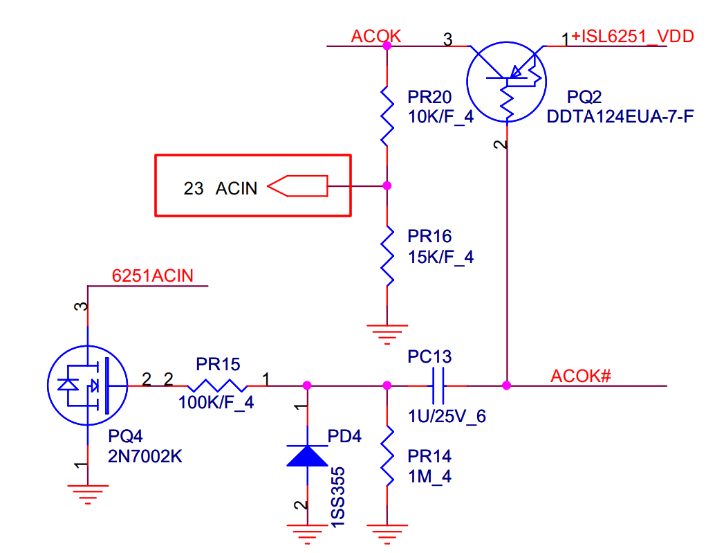
Here we find ACIN once again , but is it possible to identify its origin? We see that ACIN appears in a voltage divider formed by PR20 and PR16 . We can also see that on one side of the PR20 we have a signal called ACOK . This in turn is in the PQ2 COLLECTOR . We can also see that the ISSUER of PQ2 have a sign + ISL6251_VDD and the base have a sign AcOH # , pay close attention to this # .
Do you agree with me that so far you have not been able to define much? That only with this information is practically impossible to understand where this ACIN really arises ?
So let's take a closer look at this circuit. That by this time I hope you have already realized that we are on the CHARGE circuit .
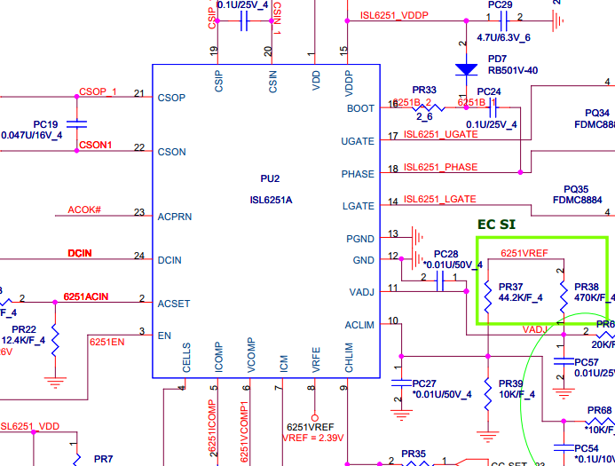
In this image we have an overview of the ISL6251A . This is the charge IC responsible for regulating the battery charge and providing charger information for the super IO .
We can notice the pins: 24 - DCIN , 2 - ACSET , 8 - VREF, 23 - ACPRN and 1 - VDD .
The basic and summarized operation of this IC is that when it receives voltage from the charger on pin 24 - DCIN , it will generate an internal reference that can be measured on pin 8 - VREF and will also generate a 5v regulator that has its output on pin 1 - VDD .
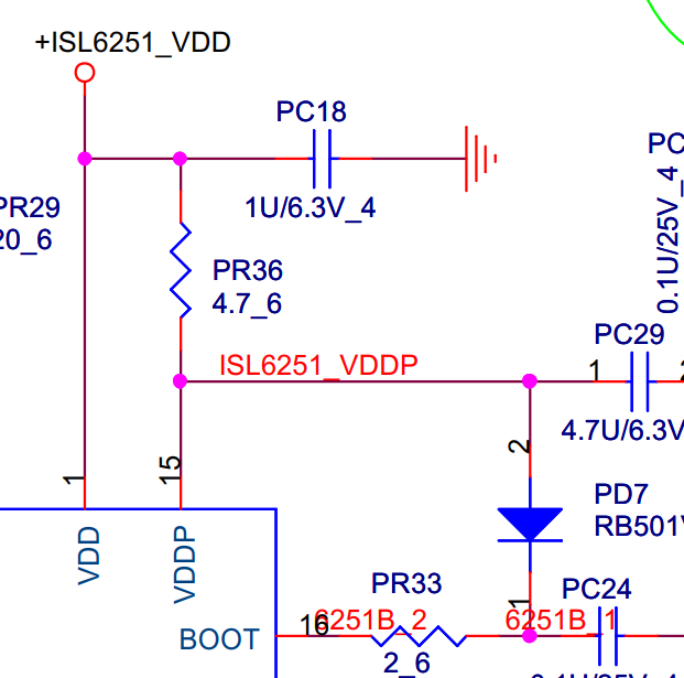
See that if the charger is connected and the charger voltage reaches pin 24 , measuring over PC18 we will have 5v , which is named +ISL6251_VDD . Now things are starting to clear up because going back to our ACIN circuit , we will already have the following condition.
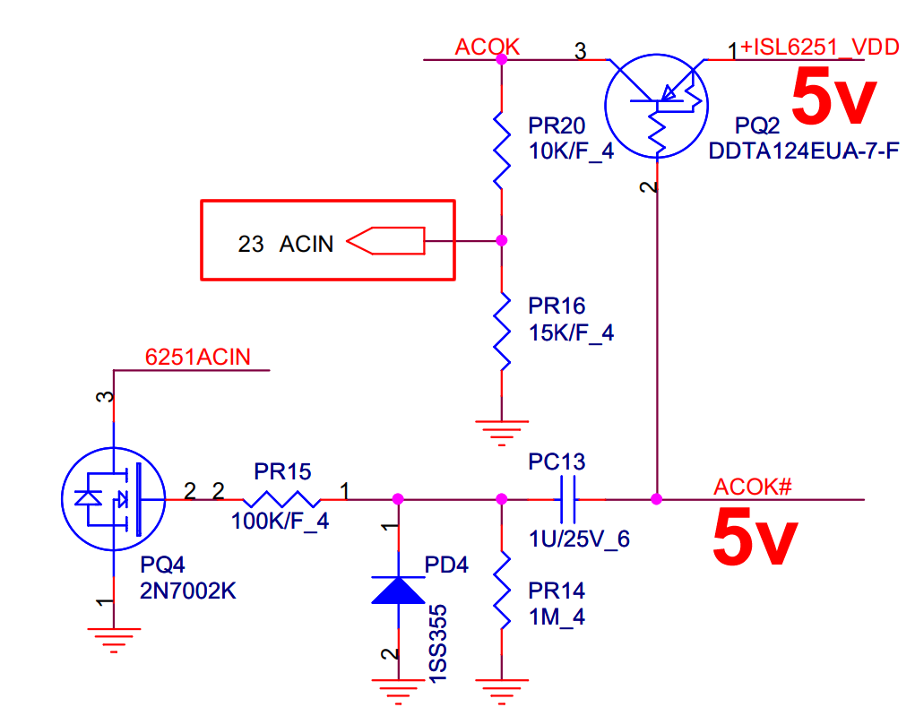
Now we know that in the EMITTER it will have the 5v , as we saw that the +ISL6251_VDD signal is actually the output of the 5v regulator of the CHARGER IC . Note that the ACOK# which is the BASE of PQ2 is with 5v . And maybe you are wondering why?
It's simple to see that the PQ2 is actually a digital transistor and that it has two resistors interconnecting EMITTER and BASE . So, up to this exact moment of the explanation, we can assume that this circuit is like this.
But Edson and ACOK without the # as it appears?
Calm down, let's get there.
For that we will return to the CI of CHARGER .
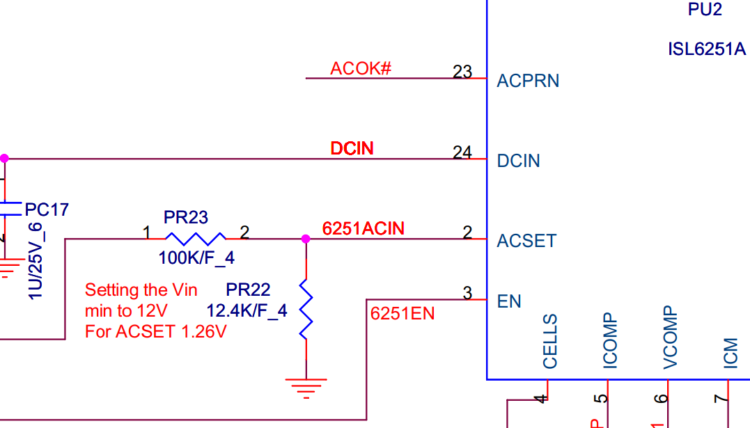
See that following our analysis on pin 23 - ACPRN and that it is connected to the ACOK# signal we will have the 5v , because this pin is connected to the base of the PQ2 .
And see that on pin 2 - ACSET . We have a voltage divider. What this splitter does is it takes a sample of the charger voltage and reports it to pin 2 . When this sample voltage reaches 1.26v pin 23 is internally grounded, so any voltage on it is grounded. This pin is what we call an OPEN-DRAIN .
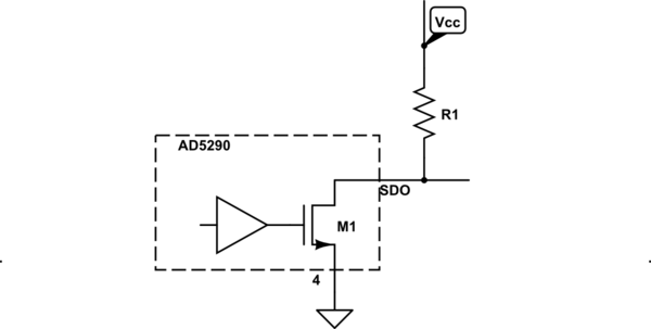
The image above demonstrates the characteristic of an OPEN-DRAIN circuit .
Assuming that pin 2 of the CHARGER is above 1.26v and that pin 23 is now connected to ground we can go back to the ACIN circuit and see how it is.
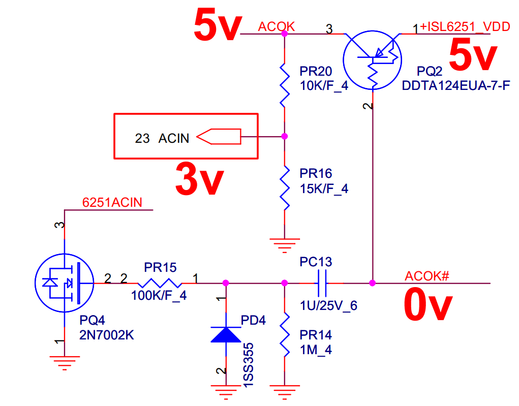
Remember that I asked you to pay attention to the # of the ACOK# sign . Well, ACOK# is an ACTIVE LOW signal , so while it was at 5v it wasn't present in the circuit. Now with pin 23 grounding , ACOK# is 0v and is therefore active. Thus, PQ2 which is a PNP and now has its emitter more polarized than its BASE conducts and finally we can witness the appearance of the ACOK signal without # . I mean he is a ACTIVE HIGHand therefore must have a value greater than zero to be active. As we saw here that it came from driving the PQ2 we can say that it has approximately 5v . Those same 5v go through the splitter and result in approximately 3v . And now the ACIN signal appears . And with that we can say that although on pin 86 of the super IO the arrow is leaving, this signal does not leave there.
Well I think that was it. Please be sure to comment what you think of this article, share it in your groups to help more friends understand this circuit.
I
make it clear that in real measurements the values can indeed undergo
some slight changes and that I am not the owner of reason. So if you disagree with some information in this article, comment there and help me to enrich this content.


No comment